As 5G, autonomous vehicles, and other emerging technologies shape the future of semiconductor demand, advanced packaging for semiconductor wafers could be key to creating value for manufacturers, according to research by senior partner Ondrej Burkacky and coauthors. Since 2000, three major advanced-packaging techniques have become commercially available and offer promising solutions for higher-performing chips: wafer level, 2.5-D stacking, and 3-D stacking.
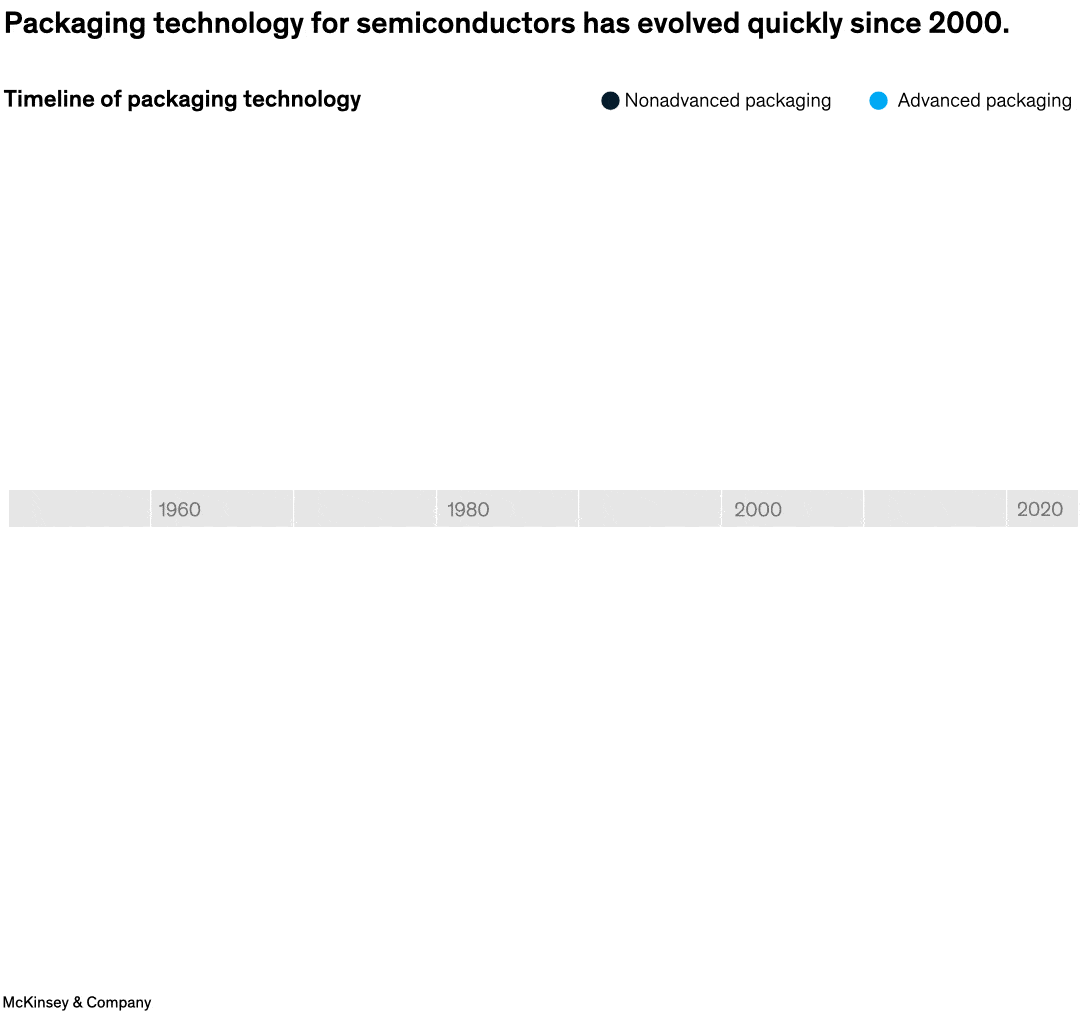
Image description:
A diagrammatic illustration shows the change in packaging technology for semiconductors from 1950–2020. Five points in time are highlighted, with the first 2 points designated as nonadvanced packaging and the remaining 3 designated as advanced. Each includes an associated diagram illustrating the semiconductor packaging of the day. The text accompanying each illustration is as follows: 1950: wire bonding; uses fine wire to connect the semiconductor chip to the printed circuit board (PCB). 1995: flip chip; connects the chip to the PCB with solder bumps and, usually, an integrated-circuit substrate. 2000: wafer level; chips are packaged as part of the wafer using a redistribution layer (RDL) rather than individually sliced. 2010: 2.5-D stacking; chips are indirectly attached on the package substrate through an interposer layer of RDL, silicon bridge, through-silicon via (TSV), or glass. 2015: 3-D stacking; multiple chip layers are stacked rather than laterally connected, with or without interposers, and bonded using TSV or other material such as copper.
End of image description.
To read the article, see “Advanced chip packaging: How manufacturers can play to win,” May 24, 2023.